- 您现在的位置:买卖IC网 > Sheet目录39246 > LM2685MTCX/NOPB (NATIONAL SEMICONDUCTOR CORP) SWITCHED CAPACITOR REGULATOR, 180 kHz SWITCHING FREQ-MAX, PDSO14
LM2685
Dual Output Regulated Switched Capacitor Voltage
Converter
General Description
The LM2685 CMOS charge-pump voltage converter oper-
ates as an input voltage doubler, +5V regulator and inverter
for an input voltage in the range of +2.85V to +6.5V. Five low
cost capacitors are used in this circuit to provide up to 50mA
of output current at +5V (± 5%), and 15mA at 5V. The
LM2685 operates at a 130 kHz switching frequency to re-
duce output resistance and voltage ripple. With an operating
current of only 800A (operating efficiency greater than 80%
with most loads) and 6A typical shutdown current, the
LM2685 is ideal for use in battery powered systems. The
device is in a small 14-pin TSSOP package.
Features
n
+5V regulated output
n
Inverts V
05(+5V) to VNEG(5V)
n
Doubles input supply voltage
n
TSSOP-14 package
n
80% typical conversion efficiency at 25mA
n
Input voltage range of 2.85V to 6.5V
n
Independent shutdown control pins
Applications
n
Cellular phones
n
Pagers
n
PDAs
n
Handheld instrumentation
n
3.3V to 5V voltage conversion applications
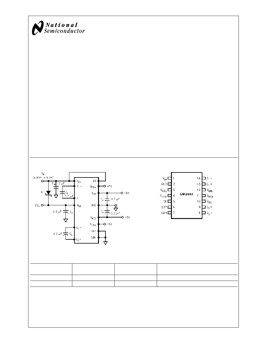
Typical Application and Connection Diagram
10110001
10110002
14-Pin TSSOP
Ordering Information
Order Number
Package Type
NSC Package
Drawing
Supplied As
LM2685MTC
TSSOP-14
MTC14
94 Units, Rail
LM2685MTCX
TSSOP-14
MTC14
2.5k Units, Tape and Reel
May 2000
LM2685
Dual
Output
Regulated
Switched
Capacitor
V
oltage
Converter
2004 National Semiconductor Corporation
DS101100
www.national.com
发布紧急采购,3分钟左右您将得到回复。
相关PDF资料
LM2686MTCX/NOPB
SWITCHED CAPACITOR REGULATOR, 180 kHz SWITCHING FREQ-MAX, PDSO14
LM2787BPX/NOPB
0.01 A SWITCHED CAPACITOR REGULATOR, 450 kHz SWITCHING FREQ-MAX, PBGA8
LM2787TP/NOPB
0.01 A SWITCHED CAPACITOR REGULATOR, 450 kHz SWITCHING FREQ-MAX, PBGA8
LM2787BP/NOPB
0.01 A SWITCHED CAPACITOR REGULATOR, 450 kHz SWITCHING FREQ-MAX, PBGA8
LM285AH-1.2
1-OUTPUT TWO TERM VOLTAGE REFERENCE, 1.235 V, MBCY2
LM185AYH-1.2
1-OUTPUT TWO TERM VOLTAGE REFERENCE, 1.235 V, MBCY2
LM185AH-1.2
1-OUTPUT TWO TERM VOLTAGE REFERENCE, 1.235 V, MBCY2
LM285BEOA-2.5713
1-OUTPUT TWO TERM VOLTAGE REFERENCE, 2.5 V, PDSO8
相关代理商/技术参数
LM2686MTC
制造商:Texas Instruments 功能描述:VOLT CONVERTER SMD 2686 TSSOP14
LM2686MTC
制造商:Texas Instruments 功能描述:VOLT CONVERTER SMD 2686 TSSOP14
LM2686MTC/NOPB
功能描述:IC REG SWITCHED CAP DBL 14-TSSOP RoHS:是 类别:集成电路 (IC) >> PMIC - 稳压器 - DC DC 开关稳压器 系列:- 产品培训模块:Lead (SnPb) Finish for COTS
Obsolescence Mitigation Program 标准包装:1 系列:- 类型:降压(降压) 输出类型:固定 输出数:1 输出电压:3.3V 输入电压:4.5 V ~ 24 V PWM 型:- 频率 - 开关:- 电流 - 输出:125mA 同步整流器:无 工作温度:-40°C ~ 85°C 安装类型:表面贴装 封装/外壳:SOT-23-6 包装:Digi-Reel® 供应商设备封装:SOT-6 其它名称:MAX1836EUT33#TG16DKR
LM2686MTCX/NOPB
功能描述:IC REG SWITCHED CAP DBL 14-TSSOP RoHS:是 类别:集成电路 (IC) >> PMIC - 稳压器 - DC DC 开关稳压器 系列:- 产品培训模块:Lead (SnPb) Finish for COTS
Obsolescence Mitigation Program 标准包装:1 系列:- 类型:降压(降压) 输出类型:固定 输出数:1 输出电压:3.3V 输入电压:4.5 V ~ 24 V PWM 型:- 频率 - 开关:- 电流 - 输出:125mA 同步整流器:无 工作温度:-40°C ~ 85°C 安装类型:表面贴装 封装/外壳:SOT-23-6 包装:Digi-Reel® 供应商设备封装:SOT-6 其它名称:MAX1836EUT33#TG16DKR
LM2687LD
制造商:Texas Instruments 功能描述:
LM2687LD/NOPB
功能描述:IC REG SWITCHD CAP INV ADJ 8-LLP RoHS:是 类别:集成电路 (IC) >> PMIC - 稳压器 - DC DC 开关稳压器 系列:- 产品培训模块:Lead (SnPb) Finish for COTS
Obsolescence Mitigation Program 标准包装:1 系列:- 类型:降压(降压) 输出类型:固定 输出数:1 输出电压:3.3V 输入电压:4.5 V ~ 24 V PWM 型:- 频率 - 开关:- 电流 - 输出:125mA 同步整流器:无 工作温度:-40°C ~ 85°C 安装类型:表面贴装 封装/外壳:SOT-23-6 包装:Digi-Reel® 供应商设备封装:SOT-6 其它名称:MAX1836EUT33#TG16DKR
LM2687LDX
功能描述:电荷泵 RoHS:否 制造商:Maxim Integrated 功能:Inverting, Step Up 输出电压:- 1.5 V to - 5.5 V, 3 V to 11 V 输出电流:100 mA 电源电流:1 mA 最大工作温度:+ 70 C 封装 / 箱体:SOIC-8 Narrow 封装:Tube
LM2687LDX/NOPB
功能描述:电荷泵 RoHS:否 制造商:Maxim Integrated 功能:Inverting, Step Up 输出电压:- 1.5 V to - 5.5 V, 3 V to 11 V 输出电流:100 mA 电源电流:1 mA 最大工作温度:+ 70 C 封装 / 箱体:SOIC-8 Narrow 封装:Tube